Versal Adaptive SoC:デザインメソドロジー
| カテゴリ画像 | Courseへのリンク | 日程 | 会場、受講料 | 状況 | category | 開催月 | 締切時間 | Flag |
|---|---|---|---|---|---|---|---|---|
| Vivado.png | Vivado Design Suite でのFPGA設計導入 | 4月4日(木)-5日(金) 申込締切日:3/26 10:00~17:30 | オンライン TC:8TC 現金:¥107,800 | 開催中止 | FPGAデバイス&ツールコース | 2024年4月 | 202403261700 | 0 |
| embe.png | Zynq SoC システムアーキテクチャ | 4月4日(木)-5日(金) 申込締切日:3/26 10:00~18:00 | オンライン TC:8TC 現金:¥107,800 | 開催中止 | エンベデッドコース | 2024年4月 | 202403261700 | 0 |
| Vivado.png | Vivado Design Suite を使用したArtix-7 FPGA設計・開発入門 | 4月9日(火) 申込締切日:3/29 10:00~17:30 | 新横浜(hdLab) TC:4TC 現金:¥53,900 | 1566 | FPGAデバイス&ツールコース | 2024年4月 | 202403291700 | 1 |
| embe.png | ARTYを使用したMicroBlaze開発入門 | 4月10日(水) 申込締切日:4/1 10:00~17:30 | 新横浜(hdLab) TC:4TC 現金:¥53,900 | 開催中止 | エンベデッドコース | 2024年4月 | 202404011700 | 0 |
| Vivado.png | [Verilog] Xilinx/Vivadoツールを使ったRTL設計初級 | 4月11日(木)-12日(金) 申込締切日:4/2 10:00~18:00 | オンライン TC:8TC 現金:¥107,800 | 1568 | FPGAデバイス&ツールコース | 2024年4月 | 202404021700 | 1 |
| Vivado.png | Vivado Design Suite でのUltraFast設計手法 | 4月15日(月) 申込締切日:4/4 10:00~17:30 | オンライン TC:4TC 現金:¥53,900 | 1569 | FPGAデバイス&ツールコース | 2024年4月 | 202404041700 | 1 |
| Vivado.png | Vivado Design Suite でのインプリメント手法 | 4月16日(火) 申込締切日:4/5 10:00~17:30 | オンライン TC:4TC 現金:¥53,900 | 1570 | FPGAデバイス&ツールコース | 2024年4月 | 202404051700 | 1 |
| Vivado.png | Vivado Design Suite でのパーシャルリコンフィギュレーション | 4月23日(火) 申込締切日:4/12 10:00~17:30 | 新横浜(hdLab) TC:4TC 現金:¥53,900 | 1571 | FPGAデバイス&ツールコース | 2024年4月 | 202404121700 | 1 |
| AdovancedMin2.png | Zynq UltraScale+ MPSoC システムアーキテクチャ | 4月25日(木)-26日(金) 申込締切日:4/16 10:00~18:00 | オンライン TC:12TC 現金:¥132,000 | 1572 | アドバンスドコース | 2024年4月 | 202404161700 | 1 |
| Vivado.png | XILINX FPGA向けRTL設計スタイルガイドセミナー | 4月25日(木)-26日(金) 申込締切日:4/16 10:00~18:00 | 新横浜(hdLab) TC:8TC 現金:¥107,800 | 1573 | FPGAデバイス&ツールコース | 2024年4月 | 202404161700 | 1 |
| Vivado.png | Vivado Design Suite でのタイミング制約と解析 | 5月8日(水) 申込締切日:4/24 10:00~17:30 | オンライン TC:4TC 現金:¥53,900 | 1575 | FPGAデバイス&ツールコース | 2024年5月 | 202404241700 | 1 |
| Vivado.png | Vivado Design Suite でのタイミング クロージャ | 5月9日(木) 申込締切日:4/25 10:00~17:30 | オンライン TC:4TC 現金:¥53,900 | 1576 | FPGAデバイス&ツールコース | 2024年5月 | 202404251700 | 1 |
| AdovancedMin2.png | VITISアクセラレーション開発 | 5月14日(火)-15日(水) 申込締切日:5/1 10:00~18:00 | オンライン TC:12TC 現金:¥132,000 | 1577 | アドバンスドコース | 2024年5月 | 202405011700 | 1 |
| embe.png | Zynq SoC エンベデッドシステム開発 | 5月16日(木)-17日(金) 申込締切日:5/7 10:00~18:00 | オンライン TC:8TC 現金:¥107,800 | 1578 | エンベデッドコース | 2024年5月 | 202405071700 | 1 |
| AdovancedMin2.png | Zynq UltraScale+ MPSoC ハードウェアデザイン | 5月21日(火) 申込締切日:5/10 10:00~18:00 | オンライン TC:6TC 現金:¥66,000 | 1579 | アドバンスドコース | 2024年5月 | 202405101700 | 1 |
| AdovancedMin2.png | Kria KV260 入門 | 5月22日(水) 申込締切日:5/13 13:00~18:00 | 新横浜(hdLab) TC:8TC ※TCのみ | 1580 | アドバンスドコース | 2024年5月 | 202405131700 | 1 |
| CONN.png | PCI Express デザイン | 5月23日(木)-24日(金) 申込締切日:5/14 10:00~17:30 | オンライン TC:12TC 現金:¥132,000 | 1581 | 高速インターフェイスコース | 2024年5月 | 202405141700 | 1 |
| AdovancedMin2.png | Kria KV260 Vision AI | 5月28日(火)-29日(水) 申込締切日:5/17 10:00~18:00 | オンライン TC:12TC 現金:¥132,000 | 1582 | アドバンスドコース | 2024年5月 | 202405171700 | 1 |
| Vivado.png | [Verilog] Xilinx/Vivadoツールを使ったRTL設計初級 | 5月30日(木)-31日(金) 申込締切日:5/21 10:00~18:00 | オンライン TC:8TC 現金:¥107,800 | 1583 | FPGAデバイス&ツールコース | 2024年5月 | 202405211700 | 1 |
| embe.png | Embedded Systems Software Design Basic | 6月5日(水)-6日(木) 申込締切日:5/27 10:00~18:00 | 新横浜(hdLab) TC:12TC 現金:¥132,000 | 1585 | エンベデッドコース | 2024年6月 | 202405271700 | 1 |
| embe.png | Embedded Systems Software Design OS | 6月7日(金) 申込締切日:5/29 10:00~18:00 | 新横浜(hdLab) TC:6TC 現金:¥66,000 | 1586 | エンベデッドコース | 2024年6月 | 202405291700 | 1 |
| Vivado.png | タイミングクロージャテクニックPart1 | 6月6日(木) 申込締切日:5/28 10:00~17:30 | オンライン TC:6TC 現金:¥66,000 | 1587 | FPGAデバイス&ツールコース | 2024年6月 | 202405281700 | 1 |
| Vivado.png | タイミングクロージャテクニックPart2 | 6月7日(金) 申込締切日:5/29 10:00~17:30 | オンライン TC:6TC 現金:¥66,000 | 1588 | FPGAデバイス&ツールコース | 2024年6月 | 202405291700 | 1 |
| Vivado.png | IP インテグレーターツールによる設計 | 6月11日(火) 申込締切日:5/31 10:00~17:30 | オンライン TC:6TC 現金:¥66,000 | 1589 | FPGAデバイス&ツールコース | 2024年6月 | 202405311700 | 1 |
| AdovancedMin2.png | OS and Hypervisors in Adaptive SoCs | 6月11日(火)-12日(水) 申込締切日:5/31 10:00~18:00 | 新横浜(hdLab) TC:12TC 現金:¥132,000 | 1590 | アドバンスドコース | 2024年6月 | 202405311700 | |
| AdovancedMin2.png | Zynq UltraScale+ MPSoC Boot and Platform Management | 6月13日(木)-14日(金) 申込締切日:6/4 10:00~18:00 | 新横浜(hdLab) TC:12TC 現金:¥132,000 | 1591 | アドバンスドコース | 2024年6月 | 202406041700 | |
| embe.png | PetaLinuxツールを使用したエンベデッドデザイン | 6月18日(火)-19日(水) 申込締切日:6/7 10:00~18:00 | 新横浜(hdLab) TC:8TC 現金:¥107,800 | 1592 | エンベデッドコース | 2024年6月 | 202406071700 | |
| Vivado.png | Vivado Design Suite でのFPGA設計導入 | 6月20日(木)-21日(金) 申込締切日:6/11 10:00~17:30 | 新横浜(hdLab) TC:8TC 現金:¥107,800 | 1593 | FPGAデバイス&ツールコース | 2024年6月 | 202406111700 | |
| Vivado.png | Verification with SystemVerilog | 6月20日(木)-21日(金) 申込締切日:6/11 10:00~18:00 | オンライン TC:8TC 現金:¥107,800 | 1594 | FPGAデバイス&ツールコース | 2024年6月 | 202406111700 | |
| Vivado.png | Vivado ロジック解析を使用したデバッグ 基礎編 | 6月25日(火) 申込締切日:6/14 10:00~17:30 | 新横浜(hdLab) TC:4TC 現金:¥53,900 | 1595 | FPGAデバイス&ツールコース | 2024年6月 | 202406141700 | |
| AdovancedMin2.png | VitisAIプラットフォーム | 6月27日(木)-28日(金) 申込締切日:6/18 10:00~18:00 | オンライン TC:12TC 現金:¥132,000 | 1596 | アドバンスドコース | 2024年6月 | 202406181700 | |
| Vivado.png | [VHDL] Xilinx/Vivadoツールを使ったRTL設計初級 | 6月27日(木)-28日(金) 申込締切日:6/18 10:00~18:00 | オンライン TC:8TC 現金:¥107,800 | 1597 | FPGAデバイス&ツールコース | 2024年6月 | 202406181700 |
Versal デバイスを対象とした設計をするには、さまざまな AMD Versal™ アダプティブ SoC 設計手法とテクニックを使用します。 また、アプリケーションのパーティショニング、デザインのクロージャ、電源および熱ソリューションを適用してデザインのパフォーマンスを向上させる方法も学びます。
このコースの重点項目は次のとおりです。
Versal デバイスの組み込みソフトウェア開発フローのデモンストレーション
▪ 提供された設計ツールと Versal アダプティブ SoC 設計手法を使用して、複雑なシステムを作成する
▪ 電力設計マネージャー (PDM) ツールを電力見積もりに活用する
▪ システムレベルのシミュレーションとデバッグの実行
▪ Versal アダプティブ SoC システムのパフォーマンスの向上
▪ Versal アダプティブ SoC 電源および熱ソリューションの特定
【ご注意下さい】
このコースの説明は日本語で行いますが、テキストは英語となります。
従来の「Versal ACAP: アーキテクチャとメソドロジー1、2」は「アーキテクチャ」と「デザインメソドロジー」に分割されました。
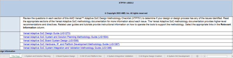
Versal Design Methodology Checklist (XTP751) TOPシート
| コース名 | Versal Adaptive SoC:デザインメソドロジー |
|---|---|
| ソフトウェアツール | ・Vivado ML Edition 2023.1 ・Vitis unified software platform 2023.1 ・PetaLinux Tools 2023.1 |
| ハードウェア | ・Architecture: Versal adaptive SoC ・Demo board: Versal VCK190 Evaluation Platform |
| トレーニング期間 | 2日間 |
| 受講料 | 1名様 12TC or 132,000円(税込) |
| 受講対象者 | ハードウエアエンジニア、ソフトウエアエンジニア、システムアーキテクト、DSPユーザー および Vesal Adaptive SoCデバイスの設計手法を学びたい方 |
| 受講要件 | ・AMD FPGA およびアダプティブ SoC に関する基礎知識 ・Vivado™ および Vitis™ ツールの基本的な知識 |
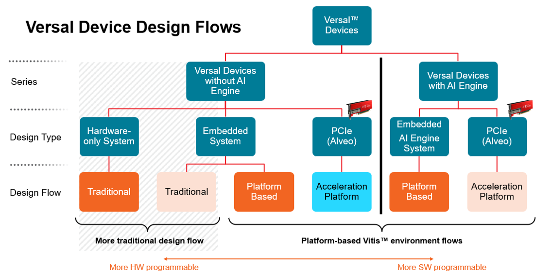
| コース内容 | ※テキストは全て英語です! Day 1 ・Board System Design Methodology Describes PCB, power, clocking, and I/O considerations when designing a system. {Lecture} ・Embedded Software Development Describes the software development environments and embedded software development flows for Versal devices. Also introduces embedded software debugging. {Lecture, Lab} ・Software Build Flow Provides an overview of the different build flows, such as the do-it-yourself, Yocto Project, and PetaLinux tool flows. {Lecture, Lab} ・Software Stack Reviews the Versal device bare-metal, FreeRTOS, and Linux software stack and their components. {Lecture} ・Security Features Describes the security features of the Versal devices. {Lecture} ・System and Solution Planning Methodology Describes design partitioning, power, and thermal guidelines. Also reviews system debug, verification, and validation planning. {Lecture} ・Application Partitioning 1 Covers what application partitioning is and how the mapping of resources based on the models of computation can be performed. {Lecture} ・Power Design Manager Discusses using the new Power Design Manager tool, including import and export functions. {Lecture, Lab} Day 2 ・Hardware, IP, and Platform Development Methodology Describes the different Versal device design flows and covers the custom platform creation process using the Vivado IP integrator, RTL, HLS, and Vitis environment. {Lecture, Lab} ・System Integration and Validation Methodology Describes different simulation flows as well as timing and power closure techniques. Also explains how to improve system performance. {Lecture} ・Configuration and Debugging Describes the configuration and debug process for the Versal devices. Also covers the Versal device debug interfaces, such as the test access port (TAP) and debug access port (DAP) controller. {Lecture} ・Overview of HSDP Describes the high-speed debug port (HSDP) in the Versal device. Also goes over the steps to use the SmartLynq+ module for high-speed debugging. {Lecture, Lab} ・Fabric Debug Explains the fabric debug features available in the Versal devices and reviews the different debug IP cores supported for the Versal devices, such as the AXI Debug Hub, AXIS ILA, and AXIS VIO. {Lecture, Lab} ・System Simulation Explains how to perform system-level simulation in a Versal device design. {Lecture, Lab} ・Power and Thermal Solutions Discusses the power domains in the Versal adaptive SoC as well as power optimization and analysis techniques. Thermal design challenges are also covered. {Lecture} |